This chipset started it all… it was the first EISA chipset produced and the one which riddled me the most. Mainly because I have two EISA boards behaving differently when it comes to expansion cards which were developed later (~1992-94) and so I suspected the Bus Controller to be the reason for all the hassle:
The Hauppauge 4860, an early EISA system and my Intel Professional Workstation (aka LP486, not yet documented on this page).
The first is using a 82350 chipset while the latter has a 82350DT. Where’s the difference? There’s no clear answer to this anywhere, so I had to do some lenghty, in-depth research.
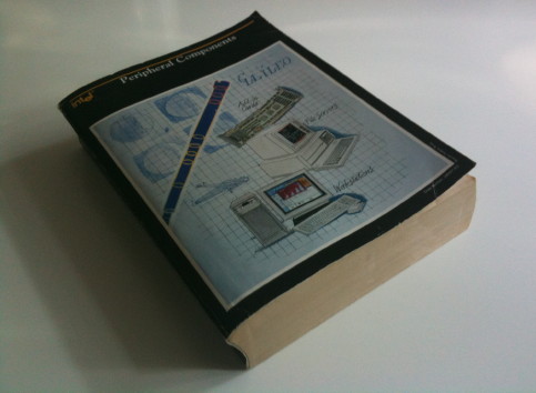
Good that I do not only collect ancient cool hardware but also some documentation, e.g. the 2″ thick Intel “Peripheral Components” handbook from 1991…

Here’s my conclusion:
- The ‘original’ 82350 Chipset -released May 1990- included just 2-3 chips: 82357, 82358(-33) and (optionally) 82352.
The 82350DT -released April 1991- consisted on 5-7 chips: 82357, 82358DT, 82359, 82351, 82352, 82353 (some of them used multiple times).
The difference between the non-DT and DT version of the 82358 seems to be the synchronous interface to the 82359 DRAM controller, which wasn’t available in the initial chipset.
Chip-by-chip round-up of the chipset:
The 82350DT EISA chip set contains 7 VLSI chips to build a complete EISA
system. It is built upon the 82350 EISA chip set utilizing the 82358DT EBC and
82357 ISP and then adds VLSI components:
- 82359 DRAM controller.
- 82353 Advanced Data Path,
- and 82351 LIOE Local IO Peripheral
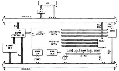
The picture below shows a 486 based system with 82350DT chip set.

The host bus connects the CPU and the memory subsystem. Tlte peripheral bus (X-bus) is an 8-bit bus to support the motherboard IO functions: keyboard, floppy and the LIOE which integrates the parallel port; and support: extemal teal time clock und serial ports. The peripheral bus is a buffered version of the 8-bit ISA bus. The memory subsection operates independent of the CPU clock. This independence is accomplished through the use of 82359’s integrated programmable delay line and the rogrammable state tracker(PST) function. The integrated programmable delay line is used to time precisely the DRAM cycle sequence to DRAM parameters. The PST resides cm the CPU module. Tite 82359/82353 reside on the motherboard. They are indifferent to the CPU/cache used. The PST converts processor cycles to a form acceptable to the 81359. This allows different CPU/ cache combinations to be connected to the same motherboard. Further, it translates CPU’s clock-dependent handshake to clock-less memory interface handshake.
Local I/O EISA Support Peripheral, lntel 82351
The 82351 supports or integrates all of the IO peripheral functions for a typical EISA system board with a minimum of external logic. lt integrates local I/O ddress decoder, EISA system configuration registers, two external serial I/O ontroller interfaces with four assignable interrupts generation, external EISA onfiguration RAM interface, parallel port interface, external floppy disk controller Interface, external keyboard (8×42) controller interface including interrupt generation, and external real time clock interface and EPROM or FLASH EPROM BIOS ROM interface. lt was available in a 132-pin PQFP (Plastic Quad Flat Pack) package.
EISA Bus Buffer (EBB), Intel 82352
The 82352 is a bus buffer IC for EISA bus system. Three 82352 chips are used in a 82350 EISA system. Only one 82352 chip is used in a 82350DT EISA system.
lt operates in three modes. ln Mode 0 it performs data latch and swap functions.
It allows swapping and assembly of data between the host and EISA/ISA buses on a byte by byte basis. In Mode 1 it provides 1 buffered path between the host data bus and DRAM with parity generation/check. Mode 2 was reserved by Intel for future use (never happened). Mode 3 provides address latching function between the host and EISA/ISA buses. The 82352 was available in 120-pin quad flat pack (QFP).
Advanced Data Path, Intel 82353
The 82353 provides advanced data path in e 82350DT EISA bus system. Two 82353 chips are used in a 82350DT EISA bus system as showed in the graph. Each 82353 is designed as a 16-bit slice. Two 82353 chips can provide parallel interface to 32, 64 or 128- bit wide memory structures to a 32-bit host and system bus.
The 82353 provides optimal 486 burst performance. Each memory cycle enerated by the address controller chip causes 128 bits of memory data to be latched in two 82353 chips. Once data is latched, these 82353 chips mux the four dwords to the destination in one wait state. The 82350DT EISA bus has 128-bit memory bus. A typical burst is 128-bit wide. and a bus with the same width
allows to read the whole burst in one memory cycle. This provides a zero wait state burst at any frequency. The 82353 was available in a 164-pin PQFP package.
Integrated System Peripheral (ISP), Intel 82357
The 82357 contains DMA controllers, interrupt controllers and programmable 16-bit counter/timers. lt provides high-performance arbitration for CPU, EISA/ISA bus masters, DMA channels and refresh. It also provides logic for generation/control non-maskable interrupts. The DMA function is provided by two inbuit 82C37A DMA controllers. These DMA controllers are connected in cascade mode to provide seven independent programmable channels. The timing control for 8-, 16- and 32-bit DMA data transfer is provided. The data transfer rate is 33MB/sec. There are two 82C59A interrupt controllers in the 82357 chip, which provide 14 independent programmable channels for level or edge-triggered interrupts. The 82357 contains five 82C54 compatible programmable 16-bit timers/counters. lt was available in a 132-pin PQFP package.
EISA Bus Controller, Intel 82358DT
The 825358DT provides an interface between 386/486 CPU and EISA bus system.
It provides EISA/ISA bus cycle compatibility with the host(CPU) bus. The 82358DT is a part of intel 82350 and 82350DT chip set. It translates host(CPU) and 82359(DRAM controller) cycles to EISA/ISA bus cycles. lt supports 8-, 16- or 32-bit DMA cycles. lt also supports host and EISA/ISA refresh cycles. lt generates control signals for advanced data path(82353) and EISA bus buffer(82351). lt was available in a 132-pin PQFP package.
DRAM Controller, lntel 82359
The 82359 is a highly integrated advanced memory controller. lt supports 386 and 486 microprocessors. Its operation is independent of speed and type of the CPU. It allows a system designer to implement a variety of CPU/cache combinations. It provides address control, refresh generation and critical DRAM timing generation. In conjunction with two advanced data path devices (82353), it acts as a highly integrated 32-bit dual ported memory controller. Its two ports (or address gateways) to main memory are: one exclusively for the host and one exclusively for EISA. This configuration of ports permits CPU activity to be isolated from EISA bus activity. It controls up to 256MB of motherboard DRAM. It supports 32-, 64- or 128-bit wide memory configurations. lt was available in a 196-pin PQFP package.
Bus Master Interface Controller, Intel 82355
The 82355 is used in an EISA add-in card (expansion board) – thus rarely found on mainboards.
It supports 16- and 32-bit burst transfers at maximum data transfer rate of 33MB/s. It also supports 32-bit non-burst and mismatched data size transfers. It automatically handles misaligned double-word data transfer with no performance penalty. It has two independent data transfer channels with 24-byte FIFOs. Expansion board timing and EISA timing operate asynchronously. The 82355 supports 32-bit EISA addressability (4GB). It integrates three interfaces:
EISA, local CPU and transfer buffer. It supports automatic handling of complete EISA bus master protocol. This includes EISA arbitration/preemption, cycle timing and execution, byte alignment, etc. Further, the 82355 supports local data transfer protocol similar to traditional DMA. It was available in a 132-pin JEDEC PQFP package.


