The IMSB430 is a rare, yet interesting and important TRAM. It’s been meant for hardware developers to easily build and test prototypes before producing actual PCBs.
Interesting enough, next to no documentation besides a sales brochure has survived. So it’s time for reverse engineering… again. This is also an official call for help – If you by any chance know more about this TRAM, please contact me!
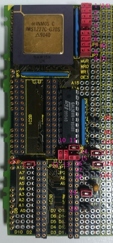
Here’s the left side of this size-4 TRAM. The other half is just the prototyping grid with lots of through holes which we can omit here.
I tried to number all jumpers on the board starting at the top – numbers in brackets are the jumper-numbers actually printed on the boards silk-screen. That numbering is a bit confusing and seems not to follow any logic.
IC connections
Buzzing through all lines from/to the GAL leads to this table so far:
| 1 ProcClkOut | 20 VCC |
| 2 A13 | 19 Mem0 (IC2B „/CE“ + JP26) |
| 3 A14 | 18 Mem1 (IC3B „/CE“ + „J20“) |
| 4 A15 | 17 1Wait (IO 2-above JP8) |
| 5 notMemCE | 16 2Wait (IO above JP8) |
| 6 WaitSEL0 (JP8) | 15 3Wait (IO below JP8) |
| 7 WaitSEL1 (JP9) | 14 SelWait (MemWait+ IO below JP9) |
| 8 Map0 (JP10) | 13 BLK0 (IO below JP10) |
| 9 Map1 (JP11) | 12 BLK1 („IO1“ below JP11) |
| 10 GND | 11 (I/OE) GNDed |
Each SRAM socket is actually a “double row”.
If you seat your SRAMs aligned to the right, they will be accessed word-wide (16bit, D0-A15). When aligned to the left, they are accessed byte-wide (8bit, D0-A7). That’s why the silkscreen print says “IC2B/IC2W“…
Jumpers
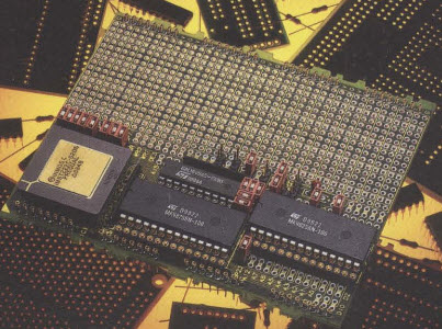
This is the official press photo. It seems to show the default jumper settings (using the full 64KB SRAM, word-access):
Some jumpers are already identified (“JP” precedes the official jumpers, “J” is my numbering):
| Jumper | description |
| 1 | MemWait (FIT=GalPin14, else ????) |
| 2 | DisIntRam (FIT=use internal RAM) |
| 3 | ProcSpeedSel0 (FIT=HoldToGnd T222) |
| 4 | MemReq (FIT=no request) |
| 5 | EventReq (FIT=no request) |
| 6 | MemBacc (FIT=word access) |
| 7 (JP6) | ProcSpeedSel2 (FIT=HoldToGnd T222) |
| 8 | BootFromRom (FIT=BootFromLink) |
| 9 (JP7) | ProcSpeedSel1 (FIT=HoldToGnd T222) |
| JP8 | Set MemWaitstate Bit0 |
| JP9 | Set MemWaitstate Bit1 |
| JP26 | Connects /OE with /CE of IC2 (upper SRAM) |
| J20 | Connects /OE with /CE of IC3 (lower SRAM) |
The external RAM access wait-states can be set with JP8/9:
JP8 + JP9 = 2 clock-cycles per MemAccess
JP9 = 3 clock-cycles
JP8 = 4 clock-cycles
none = 5 clock-cycles
To be continued…


