The US company MicroWay (also known for their NDP compiler range), presented an i860 ISA card called NumberSmasher 860.
It was available in two speed grades, costing 11698 DM (@33 MHz) or 14170 DM (@40 MHz). The needed compiler (C, Pascal or Fortran) was an 3135 DM extra.
This 16-bit ISA card featured an 40MHz i860, 4 or 8MB of ram and one INMOS OS-link controlled by a IMSC012 on a litte PCB, hiding 2 additional IMSC012 below it on the main PCB.
It is possible to connect one IMS C012 to to the ISA host bus to “feed” the Number Smasher 860 with programs and data (seedocumentation at the bottom of this page).
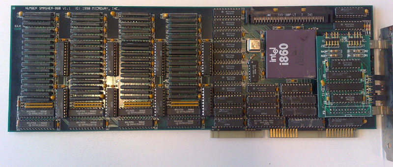
Here’s the board in its full beauty:
The left half is occupied by the 8MB RAM. The right half is all bus-logic, buffers and drivers. At the top is a very custom HD-connector – thanks to Jörg Heilmann I now know that this is the FiFo-Connector counting 100 pins. Again thanks to Jörg I also have4 pages of documentation to this connector which was designed to connect the FIFO I/O board (available as ISA and EISA version) to.
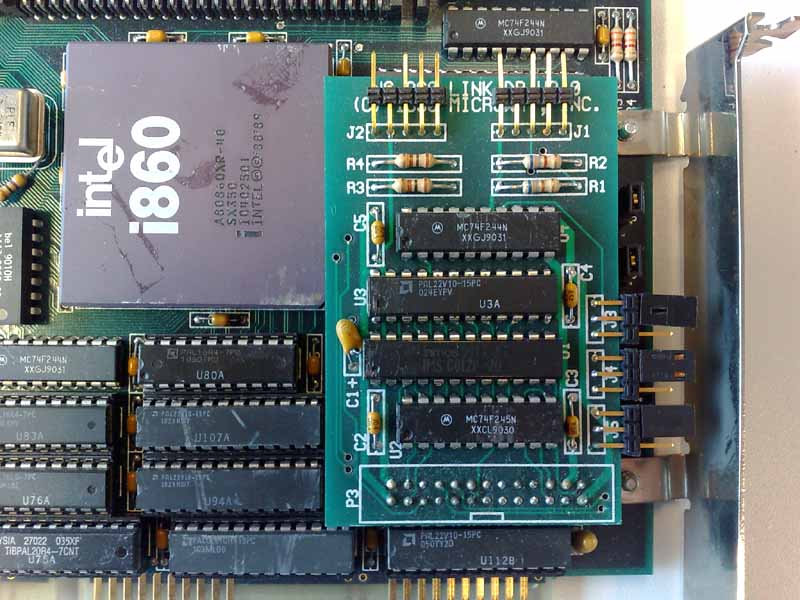
On a little separate PCB (having “LINK DR V2.0” printed on it) connected to P3 some sort of additional communication part was placed, consisting of an octal transceiver, one INMOS C012 link-adapter a PAL and an octal buffer featuring two 4-pin connectors (J1 & J2).
- J1 – GND – GND(code) – to pin 3 of J4 – to pin 3 of J3 – GND
- J2 – GND – GND(code) – to pin 16 of P3 – to pin 14 of P3 – GND
Additionally there are 3 configuration jumpers – function as far as my measurements go:
- J3 – Connects pin 18 of the board-connector (LinkIn lower onboard C012) to either LinkOut of the C012 (jumper on upper pin) or to the 4th pin of J1 (jumper on lower pin).
- J4 – Connects pin 20 of the board-connector (LinkOut lower onboard C012) to either LinkIn of the C012 (jumper on upper pin) or to the 3rd pin of J1 (jumper on lower pin).
- J5 – Linkspeed for the IMSC012 (upper is 20Mbps, lower is 10Mbps)
Documentation
As I have next to no official documentation about this board I would be very glad to hear from anybody who knows the tiniest bit about this card! AFAIK the original “manual” wasn’t bigger than 13 pages… pretty lame for a board costing as much as a small car back in those days.
Thanks to Jörg Heilmann, I got my first piece of original documentation: The 100 pin FIFO-Connector is described on these four pages. Not much but a start!
Here’s what I found out about the P3 connector on the board, having the “LINK DR” PCB plugged into it. If you have a look at the picture above, I’m start counting pins from bottom right continuing zig-zag like this:
26 oooo...oooo 2

25 oooo...oooo 1
1 – VCC
2 – CLK 5MHz
3 – Reset of the C012 (Pin 11) goes directly to the i860 reset-pin
4 – GND
5 – D7 from ISA Bus
6 – D6 from ISA Bus
7 – D5 from ISA Bus
8 – D4 from ISA Bus
9 – D3 from ISA Bus
10 – D2 from ISA Bus
11 – D1 from ISA Bus
12 – D0 from ISA Bus
13 – ???
14 – Pin 2 of the upper onboard C012
15 – ???
16 – Pin 1 of the upper onboard C012
17 – ISA Pin B8 (NoWS)
18 – Pin 2 of the lower onboard C012
19 – ???
20 – Pin 1 of the lower onboard C012
21 – MEMW to ISA
22 – MEMR to ISA
23 – ???
24 – ???
25 – VCC
26 – GND
From these findings I conclude that J2 is directly connected to the upper onboard C012 while J1 is either connected to the lower onboard C012 (J3 & 4 set to upper pins) or to the C012 on the LINK DR (J3 & 4 set to lower pins) which has its data-lines connected to the ISA bus.
On the main-card are 3 other jumpers:
- J1 & J2 – Set the connection speed of the two C012 on the card
- J3 – Select the ISA IRQ. Top down: IRQ 10, 11, 12, 15.
Everything else I have for now is a single article from the German computer magazine “c’t” (3/91,p.164 by O. Grau and A. Stiller) giving a bit more insight in the way the card works:
“Das Interface zum ISA-Bus des Hostrechners ist auf einer kleinen austauschbaren Platine untergebracht und basiert auf einem FIFO. Durch ihn geht sämtlicher I/O. Ein vergleichsweise aufwendiges Protokoll sorgt für einen recht langsamen Datentransfer, so besteht jeder Transfer aus dem Kennbyte 0 (Schreiben) oder 1 (Lesen), gefolgt von der Zieladresse (vier Bytes) und dem Datum (vier Bytes).”
The interface to the hosts ISA-bus is located on a small changeable board and is based on a FIFO [buffer]. All I/O is going through this. A comparably complex protocol is the reason for the data transfer being a bit slow. Each transfer consists of a ID-byte (0=write, 1=read) followed by the target address (four bytes) and the data (four bytes).
This “protocol” sounds very familiar to me. INMOS had the same, calling it PEEK and POKE… I’m still evaluating this, so stay tuned.
[11/05/10] Great News! I had some time and did some deeper investigation… hardware archaeology at its best 😉 So read on in the next post… it’s dissection time!


Hi, I wish that I had seen this article earlier…. I designed this entire board. I still have all the paper designs in my garage. Microway licenced the design from my employers, The University of Bath in the UK, where I am still an academic to this day. Nice article, if you want more details I probably have it in my garage. I also have about 4 of the boards still knocking around.
High Rod,
You’re right, You did design our card, and we licensed it from Bath out of our London Office, as I recall, your design used an Transputer T8 interface, that we had to add a T8 to ISA interface for. We also developed a lot of i860 software, that culminated in our QuadPuter-860 card, whose architecture employed four i860 modules each of which had 8 MB of memory running at 160 MB/sec, that all plugged into a 32MB base board, that plugged into an EISA bus, that made it possible for us to plug 5 QuadPuter-860s, into an EISA bus PCs, the problem being the cooling and power supplies that were all custom, whose fans while strong, are nowhere near as powerful as the Nvidia A-100 systems we ship today, that can each reject 400 Watts, that in a system that could hold up to 8 to 10 A400s in a 4U chassis, makes it possible to produce an air cooled system that rejects 40 KW sitting in a 44U tall rack cabinet. Are the guys I used to work with at Bath still around. Our largest market for the Number Smasher-860 was in Auatria, where it was used in an ML engagement using OCR to read and verify bank deposit slips.
Stephen Fried
President and co-founder of Microway Inc.
that closed our London office in 1993.
Wow, I’m honored to have you commenting my little writings!
Looking forward to reading Rods answer… if he’s still following.
@Rod: have you seen my NumberSmasher upgrade post? Can you remember what changes were made boor version 1.1?
Might want to know somone is selling this card on ebay right now. Cannot afford it but it has manuals and such.
https://www.ebay.com/itm/226156369268?_trkparms=amclksrc%3DITM%26aid%3D1110025%26algo%3DHOMESPLICE.COMPOSITELISTINGS%26ao%3D1%26asc%3D266917%26meid%3D4ccc8aba6a0049598b7f55b7610dc446%26pid%3D101506%26rk%3D9%26rkt%3D25%26sd%3D226152619118%26itm%3D226156369268%26pmt%3D0%26noa%3D1%26pg%3D4481478%26algv%3DAlgoIndex5SimRanker&_trksid=p4481478.c101506.m1851
Hey Paul,
Thanks for the heads-up. Yeah, I know this seller, he has lots of fine things… and yes, 500€ is a bit pricy indeed.
I’ll ask for permission to use his photos and will add a chapter for this final version of the Numbersmasher.
I came here while looking for information on what mouse is used on the Stardent Vistra/Okistation (which I own one of). This article caught my eye, because my name is also Paul and I also have a Microway Numbersmasher for sale in my ebay store, albeit mine is the 8086 variant.