This is the collection of other Transputer interfaces and cards (i.e. not from the usual suspects) I came by here and there. And no, I don’t actually own them all.
Some are rare, some are odd, may are cool and most are all three of them 😉
This post will be irregularly updated as new finds come along…
Pixar Transputer Card
Yes, that’s true. Pixar built its own Transputer interface back in the days, simply called “Render Accelerator”. Nomen es omen 😉
In constant search of raw computing power they tried out everything, eg. Intels i860 and others. It was just another logical step to try speeding-up Pixars Renderman package by using a Transputer farm. As an early adopter, they had to build their own stuff to suit their demands. Here’s a very interesting read about the long way Renderman came from and which hardware they’re were using. This article about texturing techniques is mentioning this card on pp.16.
The mentioned Jeffrey Mock was also quite busy during his Pixar days in helping Logical Systems (LSC) by writing a concurrency library for their C-Compiler.
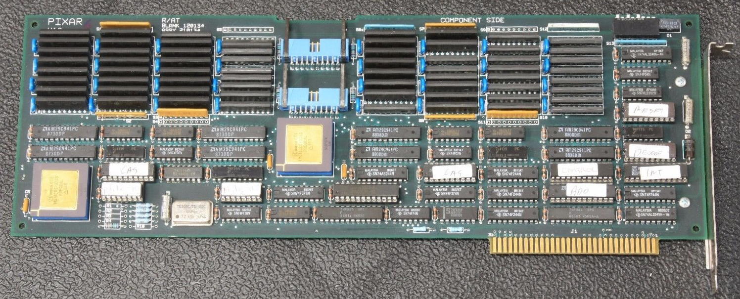
Here’s the front of the full-size 8bit ISA card – filled up to the brim.
It features two T800-20 Transputers, each having its own 4MB of RAM. Two links are facing the outside-world – I presume it’s been meant like a up- and down-link to the next card.
The rest is standard early-days ISA bus, C012, Transputer DRAM design.
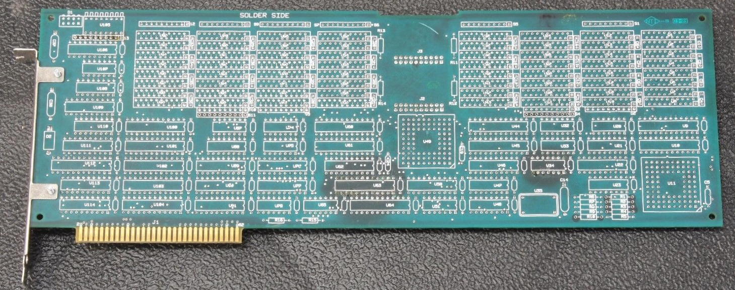
No much to say about the back side. The silkscreen is a bit uncommon, but it’s nice when it comes down to repairing… and some “burning” shows, that seemed to be the case with this specific card.
The Quintek T9
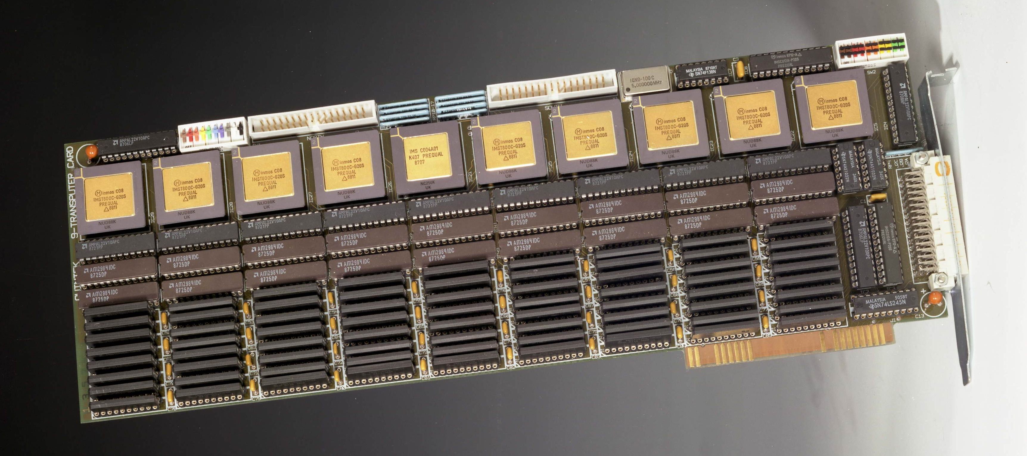
This is a very manly approach into transputing matters… don’t give me that step-by-step upgrading of an Transputer array. Just do it once and do it right 😉
Yes, that’s 9 Transputers, each with 1 or 4MB RAM and a C004 all directly soldered onto that 8-bit ISA card. It sure was expensive…
While there’s a C004 (the 6th golden IC from left), there’s no T2xx to control it. So I assume that one of the T800 is in charge to configure it… or this is done through the ISA link-interface as there are two C012 on the card,
The YARC ProTran
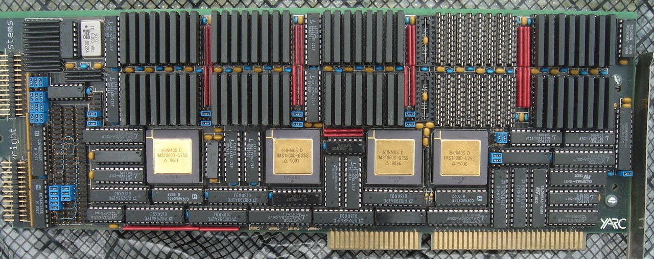
This is a fullsize 16-bit ISA card from YARC. It features 4 Transputers with the option of supporting them with a (for the time) big amount of RAM.
The ProTran board can be equipped with 1 to 4 Transputers. The root Transputer (the rightmost) can have acces to 1-16 megabytes of RAM – it’s 8 in this picture. Each of the other three can be configured with 1 to 8 MB. That was very serious stuff back then.
What’s most interesting about this card is that YARC didn’t gave much about standards and went a proprietary route in many places:
- A proprietary bus interface is said to provide a peak I/O speed exceeding 1 MB/sec
- All links, event inputs and subsystem control signals are fed to a proprietary pin-field array.
- The memory design uses a multibank and interleaving technologies to achieve zero wait state performance
All this explains the excessive use of GALs in the lower half of the card. Beside the proprietary approach the ProTran offered a compatibility mode (read: B004 interface) to use standard INMOS tools.
CSA
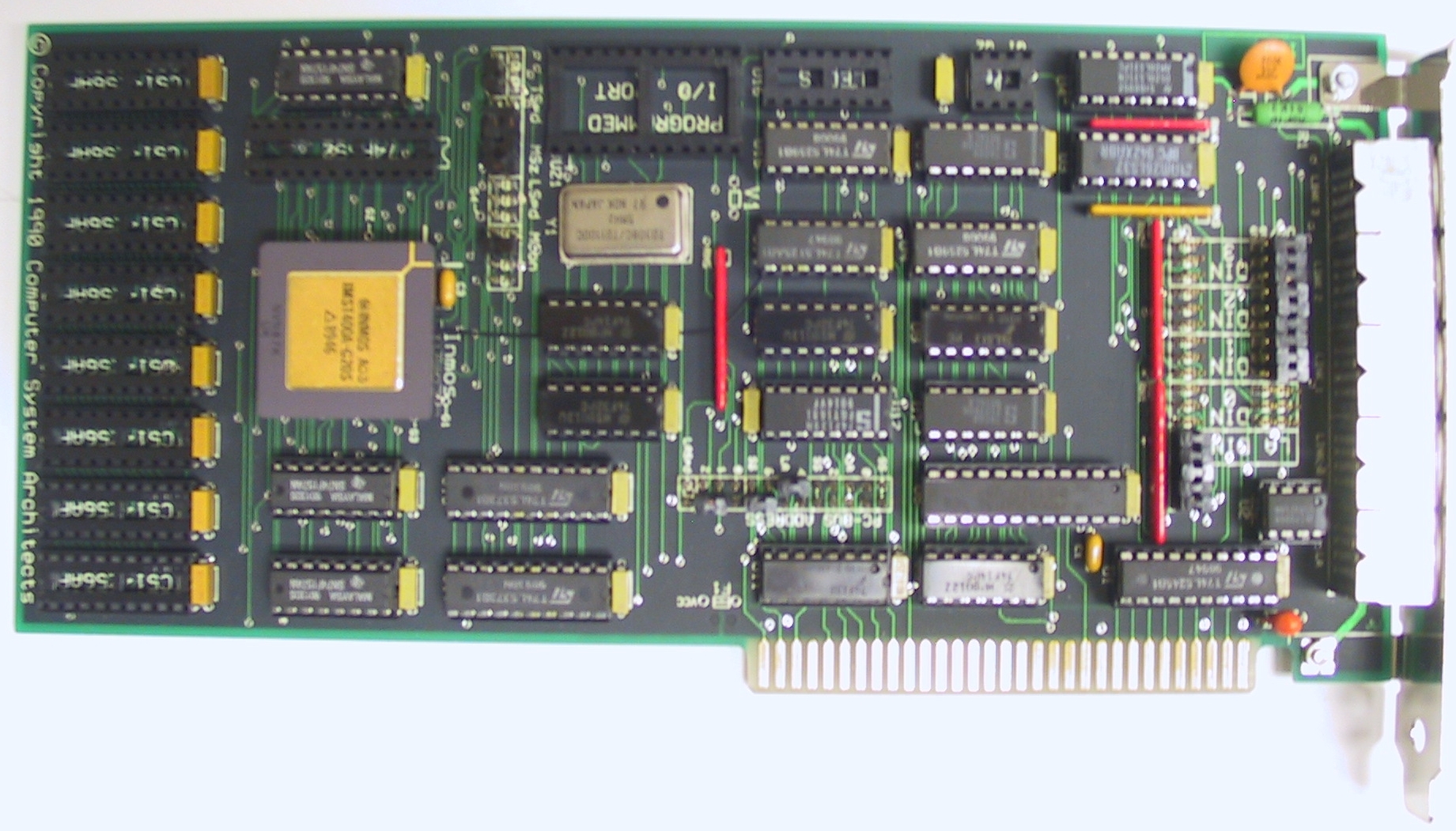
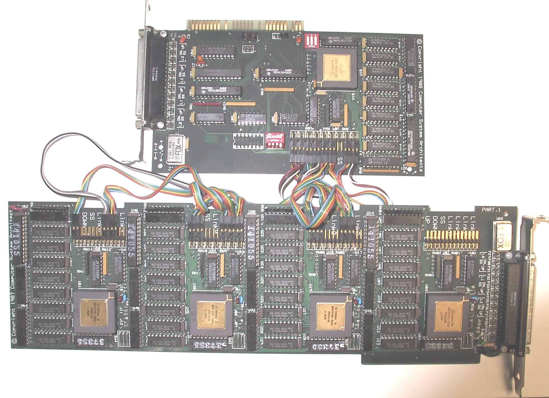
CSA (Computer Systems Architects) was big in the educational market and produced smaller, better integrated B004 compatible Transputer cards. The higher integration of DRAM parts allowed half-length ISA cards meant for evaluation or as a starting point for building bigger systems later.
(The following pictures are courtesy “the PCPUTER” page. Permission to repost them were kindly granted)
Meet the “Transputer Kit PC Card” – They came bundled with a slightly restricted version of the Transputer Toolset, together with a great manual which described lots of different programming and hardware interfacing lab-type experiments. These cards used standard multi-pin circular DIN connectors/cables to route the link and reset signals, and provided the first hands-on introduction to distributed parallel processing for many people. They included a “budget” T400A 32 bit non-floating point processor, and off-processor memory was an option
This is th PART.1 four processor board – mainly a carrier for CSAs proprietary Transputer Modules (like INMOS’ TRAMs), and the single processor PART.2 board featuring a PC interface.
The “Gerlach card”
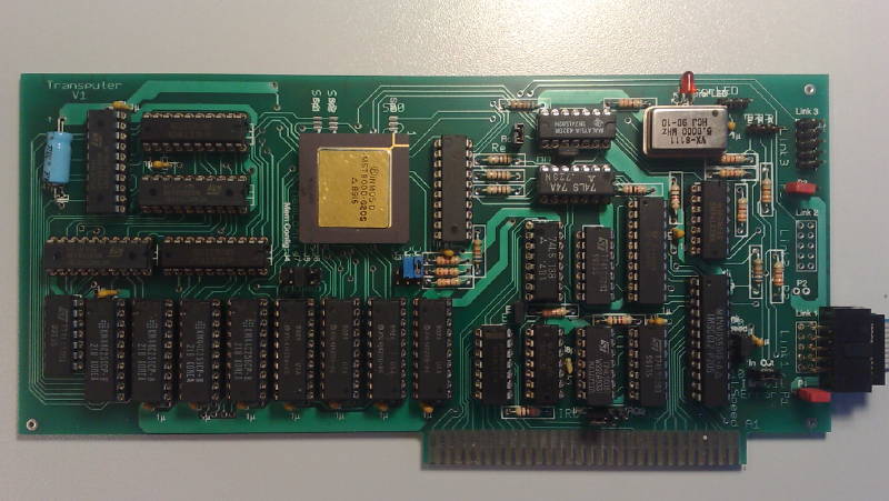
The card from the book “Das Transputerbuch” from A. Gerlach is a typical example. It has its own post on this page.<
Very simple design but only 2 layers and completely documented in the book.
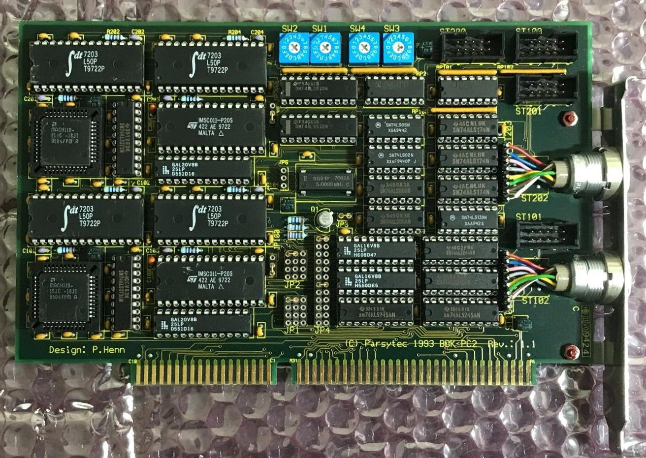
Parsytec BBK PC-2
As ususal, Parsytec did things a bit different than most others.
Their ISA interface “BBK PC-2” has two RS422 interfaces using their ‘standard’ Lemo connectors (see the the post about the x’plorer for more about these)
All Parsytec interfaces, no matter which bus-system were called BBK and having a number attached, telling you how many link interfaces were provided, e.g. the Sun SBUS card was called BBK-S4…
Like the HEMA card, this one has SRAM buffers, too. Also it looks like it’s using a 16-bit interface to the ISA bus.
Ingenieurbüro Ingo Mohnen (aka “IB Mohnen”)
This “engineering office” is pretty unknown in the already small Transputer community, even more outside Germany.
But they did very sophisticated Transputer interfaces. Actually they were the OEM for Parsytecs PCI BBK but offered other cards, too.
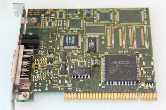
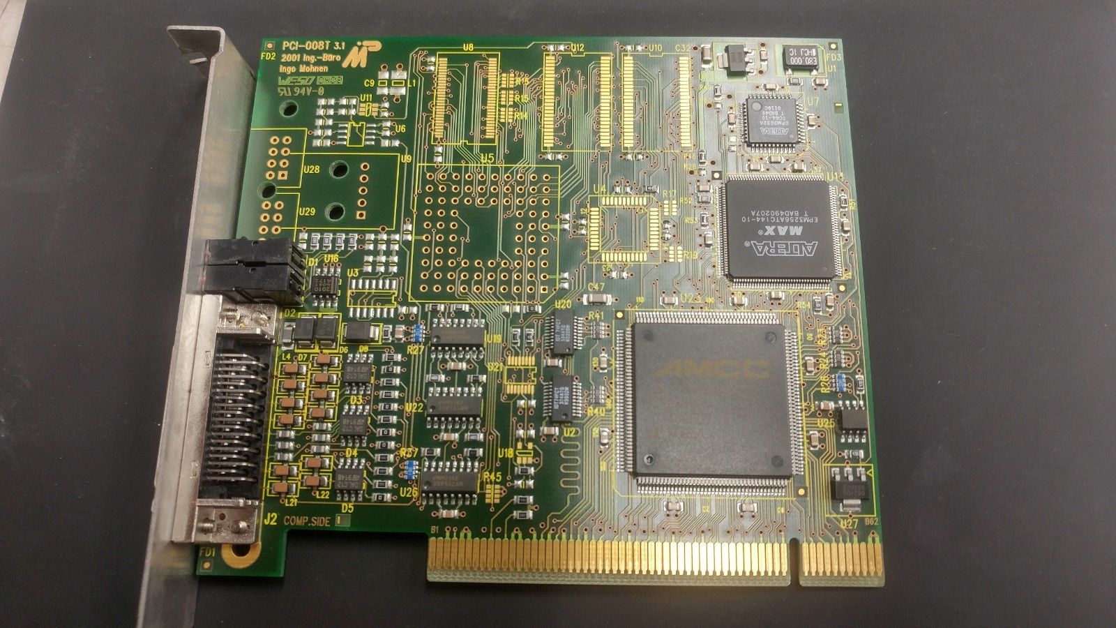
For example the PCI-008 series. Obviously a IMSB008 for the PCI bus. I have pictures of the V2.0:
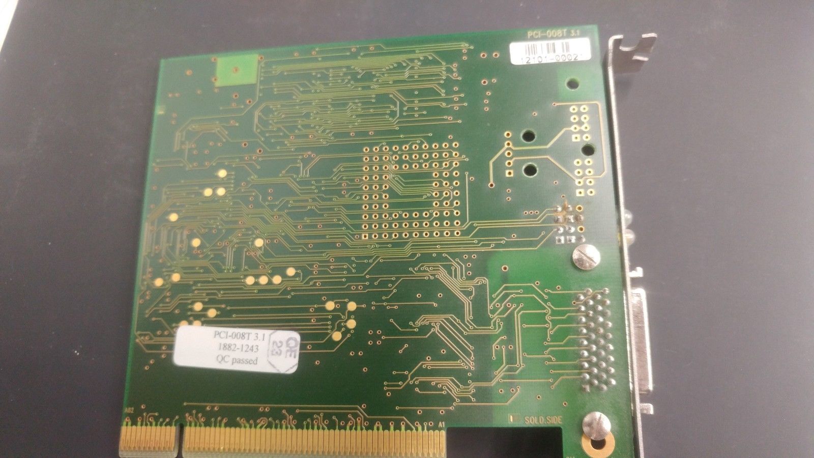
…and V3.1:
Both versions seem to be primarily meant as OS-Link interface, while they offer space for an onboard Transputer and RAM both weren’t populated with these.
V3.1 also seem to implement the C011 into the FPGA while switching back to a PGA Transputer while having used a TQFP package in version 2.
Then there was the already mentioned BBK line of cards. Starting with the BBK-PCI light of which I don’t have a better picture than Ram does on his page (Fun fact: Also Sundance OEM’ed this card from IB Mohnen). Basically it’s a IMSB004 compatible interface for PCI. Sweet, want one!
The bigger brother is the BBK-PCI, featuring 4 full blown OS-Links and acting as PCI bus-master. Definitely the high-end of PCI link-interfaces. I do own one of these but need to make some nice photos… so in the meantime use the link to Rams page 😉

I found this device some time ago:
https://dl.dropboxusercontent.com/u/86776301/DSC_0969.JPG
https://dl.dropboxusercontent.com/u/86776301/DSC_0970.JPG
https://dl.dropboxusercontent.com/u/86776301/DSC_0972.JPG
Can you help me ID it? Hit me with email if possible.
Hi ‘aop’,
This seems to be an unknown, early Transputer card from “Micropar Inc.” simply called “T4” (Rev 1A) – that’s all taken from the last picture of yours.
There are no docs on the web as far as I can see – but the design is pretty standard:
Each Transputer has 4 (pretty slow) SIPP RAM modules totaling in 1MB per T.
At the far right, an IMSC012 hints towards a B004 compatible bus interface – so give ispy a try.
The empty space for an Motorola 68230 parallel interface/timer is interesting and a first for me. Never saw that in a Transputer design.